UNIT-II MICROCONTROLLER NOTES
Unit: 2
Micro Controller Architecture
**Explain the overview of 8051
microcontroller.
The microcontroller is a
programmable IC manufactured by VLSI technique and capable of performing
arithmetic and logical operations.
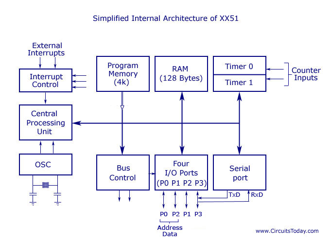
The basic functional blocks of a
microcontroller are ALU, Flag register, Register array, program counter (PC),
Instruction decoding unit, timing and control unit, RAM memory, EPROM/EEPROM
memory, parallel I/O port, serial I/O port, programmable timer, ADC and DAC.
But all the microcontrollers may not have all the blocks.
In microcontroller ALU performs arithmetic and
logical operations. Flag register : The
various conditions of the result are stored as status bits in flag register. Register array & Internal
RAM memory are used as
temporary storage device for storing temporary data during execution of a
program.
EPROM/EEPROM: The program codes and permanent data are stored in
EPROM/EEPROM.
In microcontroller based systems
external memory is provided when internal memory is not sufficient.
Most of the microcontroller based
systems, the program and data are stored in the internal memory of the microcontroller itself.
Program counter : The program counter generates the address of the
instructions to be fetched from the memory and send through internal bus to the
memory.
If the instruction to be fetched
is stored in external memory then the address is send through I/O ports to
external memory. Because the microcontrollers communicate with external world
only through I/O ports.
The memory will send the
instruction codes, which are decoded by instruction
decoding unit and send information to timing and control unit.
The timing & control unit will generate the necessary control
signals for internal and external operation of the microcontroller.
The parallel and serial I/O ports
are used for interfacing I/O devices like switches, keyboard, LCD/LED, ADC, DAC
etc and also for any other input/output operations.
The micro controllers does not have dedicated external address and
data bus. Therefore for interfacing any
additional peripheral devices, the external address and data buses are
formed only by using port lines.
The microcontrollers with
internal ADC can directly accept analog signals for processing. Like wise the
microcontrollers with internal DAC can directly generate analog signals
for controlling analog devices.
The programmable timer can be
used for time based operations and it can also be used as a counter.
** Define the features of 8051 Microcontroller.
The features of the
8051 family are :
·
4096 bytes On-Chip program memory.
·
128 bytes On-Chip data memory.
·
Four register banks.
·
128 user-defined software flags.
·
64 K bytes each program and external
RAM addressability.
·
One micro second instruction cycle
with 12 MHz crystal.
·
32 bi directional I/O lines
organized as four 8-bit ports.
·
Multiple mode, high-speed
programmable serial port.
·
Two multiple mode, 16-bit
Timers/Counters.
·
Two-level prioritized interrupt
structure.
·
Full depth stack for subroutine
return linkage and data storage.
·
Direct byte and bit addressability.
·
Binary or decimal arithmetic.
·
Signed over flow detection and
parity computation.
·
Hardware multiple and divide in 4 µsec.
·
Integrated Boolean processor for
control applications
·
Upwardly compatible with existing
8084 software.

** Explain 8051 micro controller pin diagram or pin
description.
The INTEL 8051 is an 8 bit microcontroller
with 128 byte internal RAM and 4 Kbyte internal ROM. The 8031 is same as 8051
except that it does not have internal ROM .
The 8051 is a 40 pin DIP with +5V
supply. Its maximum internal clock frequency rating is 12 MHz. The signals
shown with in brackets are alternate functions of port pins.
The 8031/8051 microcontroller has 32 I/O pins
as four 8 –bit parallel ports. i.e
port-0, port-1, port-2 & port-3 .
These ports can also be used as 8 no.of 1-bit port. Except port -1 all other
ports has alternate functions.
When 8051 is connected to
external memory then port-0 will works as multiplexed low byte address (or)
data lines. i.e ADo--AD7.
Port—2 works as high byte address
lines . (A8—A15) by using these 16 address lines
microcontroller accesses 64 Kbytes external memory. i.e 2 16 =64 K.
The external memory is
organized as two banks of 64 Kb one for program/code and the other for data. Port—3 works as a control signals.
PSEN is used to read program memory, RD is used to
read data memory & WR is used to write the data memory.
When two external memory banks
are not used (desirable ), then PSEN and
RD should be externally ANDed to provide a single read control signal.In such
cases the controller will access a common memory space for program and data.
When microcontroller is
connected to external memory then ALE (pin) is used to demultiplex the low byte
address or data using an external latch. The o/p signal on the ALE pin is clock
signal with one—sixth of (crystal) frequency (or) internal clock frequency.
When there is no external memory
then ALE is used for external I/O devices.
EA pin is used as external program
memory access control when the microcontroller will access program from
external memory then EA pin is connected ground.
During programming mode of internal PROM/ROM EA is used to supply
programming voltage (+12V).
XTAL1 & XTAL2
is used to generate a external clock for the microcontroller. (i.e
12MHz).
RST is used to reset the
microcontroller to bring known state. For proper Reset atleast two machine
cycles are required.
By giving this signal all the
internal registers are cleared. The port Latches, Stack pointer, SBUF register
& internal RAM is not effected by reset.
The 8051 has 5 interrupts.
In this two are external interrupts these are intiated by INTO & INTI pins.
Three are internal interrupts these are intiated by timer—0,timer—1 and serial
ports.
All the interrupts of
8031/8051 are maskable & vectored interrupts.
§
Pin-40 : (
Vcc) Usually it is +5V DC.
§
Pins 32-39: Known
as Port 0 (P0.0 to P0.7) – the alternating work of these pins are lower order address and data bus signals.
These signals are used for external
memory interfacing. External pull up resistors are required to function this
port as I/O.
§
Pin-30:- (ALE):
Address Latch Enable is used to de multiplex the address-data signal of port 0
(for external memory interfacing.) Two ALE pulses are available for each
machine cycle.
§
Pin-31:- EA/
External Access input is used to enable or disallow external memory interfacing.
If there is no external memory requirement, this pin is connecting
to Vcc.
§
Pin- 29:- PSEN
or Program Store Enable is used to read signal from external program memory.
§
Pins- 21-28:- are
work as Port 2 (P 2.0 to P 2.7) –and alternating work of this pins are higher order address bus signals.
§
Pin 20:-
Vss – it represents ground (0 V) connection.
§
Pins 18 and 19:- Used
for interfacing an external crystal to provide system clock.
§
Pins 10 – 17:- are
used as Port 3. This port also serves some other functions like interrupts,
timer input, control signals for external memory interfacing RD and WR , serial
communication signals RxD and TxD etc. .
§
Pin 9:- RESET
pin is used to set the 8051 microcontroller to its initial values, while the
microcontroller is working or at the initial start of application. The RESET
pin must be set high for 2 machine cycles.
§
Pins 1 – 8:- are
worked as Port 1. Unlike other ports, this port does not serve any other
functions. Port 1 is an internally pulled up, quasi bi directional I/O port.

**Explain 8051 Architecture or register organization or
block working or block diagram.
The various functional blocks of
8051 are ALU, Special function Registers (SFRs), Instruction register
(IR),Program counter (PC), 128 bytes RAM, 4Kb ROM, Port latches and drivers,
oscillators, timing and control Unit.
The 8031/8051 has Harvard Architecture in
which the same address in different memory device (or) bank is used for program
and data.
8051 has two 16—bit pointers. One is Program
counter (PC). It is used as address Pointer to access program instructions and
it is automatically incremented after every byte of instruction fetch.
Second one is data pointer (DPTR). It is used
as address pointers to read/write data in data memory and it is programmable
using instructions.
By using this 16—bit pointers
we can address 216=64 Kb memory locations. Hence 8031/8051 supports
two memory banks of 64 Kb each, one for program and the other for data.
In 8051 When EA is connected to Vcc
(logic-1) the first 4 Kb of program memory is refer to internal ROM &
remaining 60Kb is to external (EPROM/RAM) memory.
When
EA is tied (connected) to ground (logic-0) then entire 64 Kb is used as
external (EPROM/RAM) memory.
The 8051 has a separate 256 bytes internal RAM
by 8- bit address. In 256 bytes, first 128 bytes are allotted to internal RAM
and the next 128 bytes are to SFR. The RAM/SFR can be accessed by MOV
instructions & external data memory (RAM) by MOV X instruction.
The
8051 has four 8-bit ports as port-0, port-1, port-2 & port-3 . Each port has a latch and driver (
or buffer ). When external memory is employed the port-0 lines will function as
multiplexed low byte address/ data lines and port-2 lines will function as high
byte address lines. Port-3 as control signals. Port-1 does not have any
alternate function. Ports are addressed as memory locations for 8- bit
operation.
There are 21 internal
registers in SFRs. The SFRs are mapped as internal data memory. The data memory
address space 80 H to FF H are reserved for SFRs. Each registers of SFR has one
byte address, some of the registers are both byte and bit addressable.
The
8051 has 8-bit ALU ,which performs arithmetic and logical operations on binary
data. The A & B registers are used to hold the input data and the result of
ALU operation.
The controller will fetch the
instructions one by one, starting from the address stored in PC & store in
IR . Which decodes the instructions and give information to timing &
control unit.
Using the information supplied
by the IR Unit the control signals necessary for internal and external
operations are generated by the timing and control unit.
The 8031/8051 has an
internal oscillator. It is sufficient if an external quartz crystal is
connected for clock generation.
By using 16-bit programmable
timer/counter they can count the number of high to low transitions of the
signal applied to the timer pins. In timer mode of operation they can
independently programmed to work in any one of the four operating modes as
Mode-0, Mode-1, Mode-2 & Mode-3.
The 8051 family of
microcontrollers has a full duplex serial port which can be programmed to work
in any one of four operating modes namely Mode-0, Mode-1, Mode-2 and Mode-3.
In Mode-0 the serial port can either receive or
transmit at fixed baud rate. In Mode-2 it can simultaneously transmit and
receive at any one of the two selectable baud rate.
In Mode-1 and Mode-2 it can
work as full duplex serial port with variable baud rate, which is programmed
using timer-1.
There are 128 bytes of RAM
inside the 8051 microcontroller with 00H to 7FH address. These 128 bytes are
divided into three different groups, as
(1) A total 32 bytes from 00H to 1FH
locations are set for register banks and stack.
(2) A total 16 bytes from locations 20H
to 2FH are set for bit- addressable RAM.
(3) A total 80 bytes from 30H to 7FH locations
are used for read and write storage or scratch pad. These 80 locations of RAM
are widely used for the purpose of storing data and parameters by 8051
programmers.
The A & B
registers are called CPU registers they are used to store the data for CPU
(ALU) operations. These are 8-bit registers of address E0H and F0H.
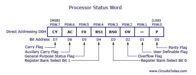
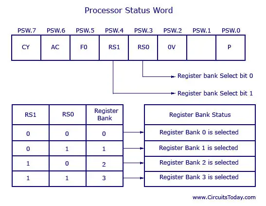
The program status word
store the status of the result of ALU operations. PSW consists of 4 Math flags
& 2 register bank select bits. The Math flags are carry, Auxiliary carry,
overflow and parity flags.

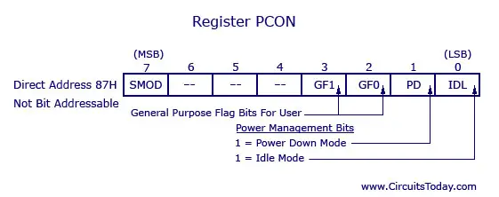
The PCON
register is used for power control and baud rate selection. It also consists of
general purpose user flags.

The TMOD
register is used to select the operating mode and the timer/counter operation
of the timers.

The TCON
register consists of timer overflow flags, timer run control bits, external
interrupt flags and external interrupt type control bits.
In reality only 5 interrupts are available in
8051 but according to data sheets there are six interrupts . Since they include
reset.
Interrupts are
RESET, Timer flag-0,Timer flag-1,INT0,INT1 , serial communication interrupts
(RI,TI). Three of the interrupts are generated automatically by internal
operations . Timer flag0,Timerflag1 and the serial port interrupt (RI&TI),
INT0&INT! are triggered by external signals.
All the interrupt functions are under the
control of the program. The programmer is able to alter control bits in the
Interrupt Enable register (IE), The Interrupt Priority register (IP) and the
Timer control register (TCON).
The IE register
is used to enable or disable the interrupts of 8051.
Interrupt Enable Register
EA
|
-
|
ET2
|
ES
|
ET1
|
EX1
|
ET0
|
EX0
|
·
EA − Global enable/disable.
·
- − Undefined.
·
ET2 − Enable Timer 2 interrupt.
·
ES − Enable Serial port interrupt.
·
ET1 − Enable Timer 1 interrupt.
·
EX1 − Enable External 1 interrupt.
·
ET0 − Enable Timer 0 interrupt.
·
EX0 − Enable External 0 interrupt.
The IP register
can be programmed to make the priority of any of the interrupt as highest Bit
addressable as IP.0 to Ip.7 .

The 8051 has a Serial data communication
circuit that uses register SBUF to hold data.

Register SCON controls data
communication register PCON controls data rates and pins RXD and TXD connect to
the Serial data network.

** Write a short note on program counter.
Program counter
is important 16-bit register in 8051. The program counter points to the address
of the next instruction to be executed. As the CPU fetches the opcode from the
program ROM. The program counter is incremented to point to the next
instruction. Program counter access program address 0000H to FFFFH. A total of
64 K bytes of code.
By applying Vcc to the RESET pin is
known as powering up. By powering up the microcontroller . The memory address
id indicated as 0000H. This means that the first opcode to be stored at ROM
address 0000H. (i.e burning of ROM).
Role of the program counter in step-by-step.
When the 8051 is
powered up, the PC has 0000H and starts to fetch the first opcode from location
0000H of the program ROM. After executing the opcode, the CPU fetches the value
and place it in destination. Now one instruction is finished. Then the program
counter is incremented to 0002H.
This process
goes on until all the instructions are fetched & executed. The PC is
automatically incremented after every instruction byte is fetched . It is the
only register that does not have an internal address.
** Explain The Memory organization in 8031/8051.
A microcontroller
based system require both EPROM and RAM. The EPROM is required for permanent
program and permanent data storage. The RAM is required for temporary data
storage and stack. The 8031/8051 has 64 K bytes program memory & 64 Kbytes
data memory.
The microcontroller can only read from program
memory. PSEN signal is used for reading the program memory. ROM/EPROM/EEPROM
are used as program memory.
The
microcontroller can read and write with data memory. RD & WR signals are
used for reading and writing the data memory. Static RAM can be used as data
memory.
In 8051
microcontroller the entire 64 Kb data memory space is external. It’s address is
0000H to FFFFH. A part from external data memory the 8051 has 256 bytes of
internal data memory in which the first 128 bytes are called RAM & next 128
byte are called SFR. The address range of SFRs & internal RAM are 00H to
FFH.
The 8051 has 4
Kb internal ROM can be mapped to first 4 Kb address space of program memory .
If EA pin is high, The address of internal ROM is 0000H to 0FFFH. The usage of
internal ROM is optional. The external program memory 60 Kb address range is
1000H to FFFFH. (remaining program memory.)
When EA pin is
low the entire 64Kb program memory 0000H to FFFFH is treated as external
memory. i.e internal 4 Kb ROM cannot be accessed.
In 8031/8051 based system, has possible to
have a single memory bank for both program and data.
To minimize the cost & when memory
requirement is less. Then single memory is used for both data & program.
When a single memory bank is provided then the
read control signal is generated by logical ANDing the PSEN and RD signals.
When a single bank is provided the system
designer has to partition the total 64Kb of address space for program and data.
Then the 256 bytes internal memory can be accessed as data memory by using
8-bit address.
The 8051 microcontroller does not provide
separate I/O addresses. Therefore in 8051 based system only memory mapped I/O
is possible. Hence some of memory address space should be reserved for I/O
devices.


** Write a short note on Data types
and directives.
The 8051 microcontroller has
only one data type. The size of each register is 8-bits.The job of the
programmer is to break down the data larger than 8-bits (00H to FFH), to be
processed by the CPU. The data types used by the 8051 can be positive (or)
Negative.
DB ( Define Byte):
The DB directive is the most
widely used data directive in the assembler. It is used to define the 8-bit
data. The numbers can be in decimal, binary, Hexa (or) ASCII formats.
The directive is the only directive that can
be used to define ASCII strings larger than two characters. Therefore it should
be used for all ASCII data definitions.
ORG 050H
Data: DB
0FCH 05H,76H
DB “SAM”.
Assembler directives:
An assembler will assemble our program and
inform to us of any errors that are found.
An assembler is a program and has instructions
just as does any program. These are called directives or Pseudo operations,
because they inform the assembler what to do with the mnemonics.
ORG (Origin)
The ORG directive is used to indicate the
beginning of the address. The number that comes after ORG can be either in Hexa
or in decimal.
ORG 500H
Data: DB 28H
ORG 518H
DB 39H
EQU (Equate):
This is used to define a constant with
out occupying a memory location. The EQU directive does not set a side storage
for a data item but associates a constant value with a data lable so that when
the lable appears in the program, its constant value will be substituted for
the lable. EQU is used for the counter constant & then the constant is used
to load the R3 register.
COUNT EQU 25
_ _ _ _ _ _ _ _ _ _ _
MOV R3, #
Count.
END
directive:
Another important Pseudo code is
the END Directive. This indicates to the assembler the end of the Source File.
The END directive is the last line of an 8051 program. Meaning that in the
source code any thing after the END directive is ignored by the assembler.
**
Write a short note on PSW register or Status register or flags.
The program status word specify the status of result after completing
the operation on ALU.
One bit status is called flag. Flags are useful for the programmer to
test the condition of the result and make decisions.
The PSW consists of 4 Math flags & 2 register bank select bits. The
Math Flags are carry, Auxiliary carry, overflow and parity flags. These flags
are selected after arithmetic and logical operations depending on the result.
The carry flag is set when the result has a carry, otherwise it is
reset. Carry flag is used in arithmetic jump,rotate and Boolean instructions.
In general, it is used to detect errors in unsigned arithmetic operations.
When there is a carry from lower
nibble to upper nibble the auxiliary carry is set. It is used for BCD
arithmetic operations.
When the result has odd parity, the parity
flag is set.
If the size of the result exceeds the size of
destination register then overflow flag is set.
Overflow flag is set when addition or
subtraction occurs or else reset. The overflow flag is only used to detect
errors in signed arithmetic operations.
RS1 and RS0 are register bank select bits. These
are used to select any one of the four register banks of the internal RAM. At
any one time the microcontroller can work with only one register bank selected
by these bits.
B1 & B5 bits are
used by the programmer for any purpose. In other words, they are user
definable.

** Write a short note on register banks and
stack.
There are 128 bytes of RAM
inside the 8051 microcontroller with 00H to 7FH address. These 128 bytes are
divided into three different groups, as
(1) A total 32 bytes from 00H to 1FH
locations are set for register banks and stack.
(2) A total 16 bytes from locations 20H
to 2FH are set for bit- addressable RAM.
(3) A total 80 bytes from 30H to 7FH
locations are used for read and write storage or scratch pad. These 80
locations of RAM are widely used for the purpose of storing data and parameters
by 8051 programmers.
Register banks in the 8051
A total 32 bytes of RAM are set
for the register banks and stack. These 32 bytes are divided into 4 banks of
registers. Each bank has 8- registers R0 to R7.
RAM locations from
00 to07 are set as Bank0
08
to 0F are set as Bank1
10
to 17 are set as Bank2 &
18 to 1F are set as Bank3.
As we
can see bank1 uses the same RAM space as the stack. This is a major problem in
programming the 8051.
We
can select the banks by using PSW bits D4 & D3 . The particular register
bank is selected by the bit addressable instructions SET B & CLR .
Eg:
SET B PSW.3
will make PSW.3 =1 and select bank.1 register.


**
Explain Stack and Stack pointer in 8051 microcontroller.
The stack is a section of RAM
used by the CPU to store information temporarily. The information may be data
or an address.
The register used to access the stack is
called the SP (Stack Pointer). The SP is only 8-bit wide from 00H to FFH.
When 8051 is powered up the SP
register contains value 07. This means that RAM location 08 is the first
location used for the stack by the 8051. Reset the stack is initialized as 07H.
For every write operation into
stack in 8051, the stack pointer is automatically incremented by one. For every
read operation from stack, the SP is automatically decremented by one.
The data stored into stack is
says as PUSH operation & receiving data is says as POP operation. The stack
in 8051 is also a LIFO stack similar to 8085.


**
Distinguish between stack and queue.
**
Explain 8051 Interrupts
In a computer program to determine
the conditions that exist in internal & external circuits are in two ways.
One way is responds to hardware signals called
interrupts, that force the program to call a subroutine.
The program associated with the
interrupt is called the interrupt service routine (ISR) or Interrupt handler.
The advantages of interrupts is that the
microcontroller can serve many devices. (not all at the same time.)
Interrupt
Service Routine:
For every interrupt, there must be
an interrupt Service Routine ( ISR). When an interrupt exist, the
microcontroller runs the ISR. For every interrupt, there is a fixed location in
memory that holds the address of its ISR.
Interrupts
in the 8051:
In reality only five interrupts are available
in 8051, but according to data sheets there are six interrupts.
(1) RESET: When the reset pin is activated,
the 8051 jumps to address location 0000. This is power-up reset.
(2) Timer
flag-0, Timer flag-1 : These
two interrupts are Timer-0 & Timer-1 interrupts. The address locations are
000BH & 001BH.
(3) INT0,
INT1 : These are
external hardware interrupts . Memory locations of INT0 is 0003H & INT1 is
0013H.
(4) Serial
communication interrupt (RI & TI) : Serial
communication interrupt is a single
interrupt to receive and transmit the memory location is 0023H.
All the interrupts of 8051 are maskable and
vectored interrupts.
Three of the interrupts are generated
automatically by internal operations . Timer flag 0, Timer flag1 and the serial
port interrupt (RI or TI).
INT0 & INT1 are triggered by external
signals.
All the interrupt functions are under the
control of the program. The programmer is able to alter control bits in the
Interrupt Enable register (IE), The Interrupt priority register (IP) and the
timer control register (TCON).
The
interrupt Enable (IE).
The IE
register is used to enable or disable the interrupts of 8051.
Interrupt Enable
Register
EA
|
-
|
ET2
|
ES
|
ET1
|
EX1
|
ET0
|
EX0
|
·
EA − (
Enable interrupt bit ) :Global enable/disable. This bit is clear to 0 by program to disable
all interrupts. Set to 1 to permit individual interrupts to be enabled by their
enable bits.
·
- − Undefined.
·
ET2 − Enable
Timer 2 interrupt. This bit is reserved for future use.
·
ES − Enable
Serial port interrupt. Set to 1 by program to enable serial port interrupt.
Cleared to 0 to disable serial port interrupt.
·
ET1 − Enable
Timer 1 over flow interrupt. Set to
1 by program to enable timer-1 overflow interrupt,. Cleared to 0 to disable
timer-1 over flow interrupt.
·
EX1 −
Enable External interrupt 1. Set to
1 by program to enable INT1 interrupt. Cleared to 0 to disable INT1 interrupt.
·
ET0 − Enable Timer 0 over flow interrupt .Set to 1 by program to
enable timer-0 over flow interrupt. Cleared to 0 to disable timer-0 over flow
interrupt.
·
EX0 − Enable
External 0 interrupt. Set to 1 by program to enable INT0 interrupt. Cleared
to 0 to disable INT0 interrupt . Bit addressable as IE.0 to IE.7
The IE register is used
to enable / disable the interrupts of 8051. The interrupts are recognized by
the controller only if they are enabled . The five interrupts of 8051 totally
or individual.
Note:1=Enable
0= Disable
Interrupt
Priority (IP) register :
The IP register can be programmed to make
the priority of any of the interrupt as highest Bit addressable as IP.0
to Ip.7 .
The 8051 has five interrupts and the
normal priority of these interrupts from highest to lowest are external
interrupt-0, Timer-0 interrupt. External interrupt-1, Timer-1 interrupt and
Serial port interrupt.
The IP register can be programmed
to make the priority of any of the interrupt as highest. Bit addressable as
IP.0 to IP.7
Note : 1 = Highest priority.
0 = Normal priority.

**Explain Timers in 8051
microcontroller.
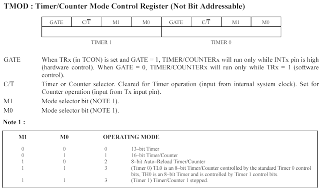
** Write a short note on Timer Mode Control Register ( TMOD) :
The TMOD register is used to select
the operating mode and the Timer/counter operation of the timers.
The lower four bits of TMOD
register is used to control Timer-0 and the upper four bits are used to control
Timer-1
The two Timers can be
independently program to operate in various modes. The TMOD register has two
separate two bit field M0 & M1 to program the
operating mode of timers.
The operating modes of
Timers are Mode-0, Mode-1,Mode-2 and Mode-3. In all these operating modes the
oscillator clock is divided by 12 and applied as input clock to timer.

Normally TR ( Timer Run ) bit in the
TCON register is used to control the clock input to Timer. ( The timer will run only if clock
input is allowed when GATE=1, then the clock input to timer is allowed only if
the signal at INT pin is high and when GATE=0 the signal at INT is ignored but
TR should be set to one.
**
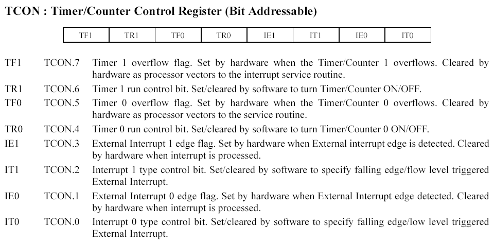
Write a short note on Timer control ( TCON) register.
The
TCON register consists of timer overflow flags, timer run control bits,
external interrupt flags and external interrupt type control bits.
The Timers in 8051 Microcontrollers
are up counters and they keep on increasing as long as clock is applied.
Therefore when clock is applied after reaching maximum value ( i.e the content
of counter is all 1’s ) . The content of counter will become zero ( i.e all 0’s
). This condition is called timer over flow .
Whenever the Timer/Counter overflows,
the TF flag is set (i.e TF=1) . The TF flag is also used as an interrupt signal
to indicate the execution of a subroutine, when the controller vectors to
subroutine the TF flag is cleared.
The TR bit is used to start/stop the
Timer/Counter, when TR bit is set to one, the Timer/Counter will start counting
and continue the counting as long as TR bit is one. The Timer/Counter will stop
counting when TR bit is cleared to zero.
When a valid external interrupt signal
is detected the IE flag is set to one, when the controller accept the external
interrupt and start processing it, the IE flag is cleared to zero. The IT bit
is used to program the type of external interrupt signal to be recognized by
the controller. The IT bit is programmed as one to recognize falling edge
triggered external interrupt and it is programmed as zero to recognize logic
low level external interrupt.

Explain
8051 Interrupts
In a computer program to determine
the conditions that exist in internal & external circuits are in two ways.
One way is responds to hardware signals called
interrupts, that force the program to call a subroutine.
The program associated with the
interrupt is called the interrupt service routine (ISR) or Interrupt handler.
The advantages of interrupts is that the
microcontroller can serve many devices. (not all at the same time.)
Interrupt
Service Routine:
For every interrupt, there must be
an interrupt Service Routine ( ISR). When an interrupt exist, the
microcontroller runs the ISR. For every interrupt, there is a fixed location in
memory that holds the address of its ISR.
Interrupts
in the 8051:
In reality only five interrupts are available
in 8051, but according to data sheets there are six interrupts
(1) RESET: When the reset pin is activated,
the 8051 jumps to address location 0000. This is power-up reset.
(2) Timer
flag-0, Timer flag-1 : These
two interrupts are Timer-0 & Timer-1 interrupts. The address locations are
000BH & 001BH.
(3) INT0,
INT1 : These are
external hardware interrupts . Memory locations of INT0 is 0003H & INT1 is
0013H.
(4) Serial
communication interrupt (RI & TI) : Serial
communication interrupt is a single
interrupt to receive and transmit the memory location is 0023H.
All the interrupts of 8051 are maskable and
vectored interrupts.
Three of the interrupts are generated
automatically by internal operations . Timer flag 0, Timer flag1 and the serial
port interrupt (RI or TI).
INT0 & INT1 are triggered by external
signals.
All the interrupt functions are under the
control of the program. The programmer is able to alter control bits in the
Interrupt Enable register (IE), The Interrupt priority register (IP) and the
timer control register (TCON).
The
interrupt Enable (IE).
The IE
register is used to enable or disable the interrupts of 8051.
Interrupt Enable
Register
|
EA
|
-
|
ET2
|
ES
|
ET1
|
EX1
|
ET0
|
EX0
|
·
EA − (
Enable interrupt bit ) :Global enable/disable. This bit is clear to 0 by program to disable
all interrupts. Set to 1 to permit individual interrupts to be enabled by their
enable bits.
·
- − Undefined.
·
ET2 − Enable
Timer 2 interrupt. This bit is reserved for future use.
·
ES − Enable
Serial port interrupt. Set to 1 by program to enable serial port interrupt.
Cleared to 0 to disable serial port interrupt.
·
ET1 − Enable
Timer 1 over flow interrupt. Set to
1 by program to enable timer-1 overflow interrupt,. Cleared to 0 to disable
timer-1 over flow interrupt.
·
EX1 −
Enable External interrupt 1. Set to
1 by program to enable INT1 interrupt. Cleared to 0 to disable INT1 interrupt.
·
ET0 − Enable Timer 0 over flow interrupt .Set to 1 by program to
enable timer-0 over flow interrupt. Cleared to 0 to disable timer-0 over flow
interrupt.
·
EX0 − Enable
External 0 interrupt. Set to 1 by program to enable INT0 interrupt. Cleared
to 0 to disable INT0 interrupt . Bit addressable as IE.0 to IE.7
The IE register is used
to enable / disable the interrupts of 8051. The interrupts are recognized by
the controller only if they are enabled . The five interrupts of 8051 totally
or individual.
Note:1=Enable
0= Disable
Interrupt
Priority (IP) register :
The IP register can be programmed to make
the priority of any of the interrupt as highest Bit addressable as IP.0
to Ip.7 .
The 8051 has five interrupts and the
normal priority of these interrupts from highest to lowest are external
interrupt-0, Timer-0 interrupt. External interrupt-1, Timer-1 interrupt and
Serial port interrupt.
The IP register can be programmed
to make the priority of any of the interrupt as highest. Bit addressable as
IP.0 to IP.7
Note : 1 = Highest priority.
0 = Normal priority.

**Explain Timers in 8051
microcontroller.

The TMOD register is used to select
the operating mode and the Timer/counter operation of the timers.
The lower four bits of TMOD
register is used to control Timer-0 and the upper four bits are used to control
Timer-1
The two Timers can be
independently program to operate in various modes. The TMOD register has two
separate two bit field M0 & M1 to program the
operating mode of timers.
The operating modes of
Timers are Mode-0, Mode-1,Mode-2 and Mode-3. In all these operating modes the
oscillator clock is divided by 12 and applied as input clock to timer.
Normally TR ( Timer Run ) bit in the
TCON register is used to control the clock input to Timer. ( The timer will run only if clock
input is allowed when GATE=1, then the clock input to timer is allowed only if
the signal at INT pin is high and when GATE=0 the signal at INT is ignored but
TR should be set to one.
**
Write a short note on Timer control ( TCON) register.

The
TCON register consists of timer overflow flags, timer run control bits,
external interrupt flags and external interrupt type control bits.
The Timers in 8051 Microcontrollers
are up counters and they keep on increasing as long as clock is applied.
Therefore when clock is applied after reaching maximum value ( i.e the content
of counter is all 1’s ) . The content of counter will become zero ( i.e all 0’s
). This condition is called timer over flow .
Whenever the Timer/Counter overflows,
the TF flag is set (i.e TF=1) . The TF flag is also used as an interrupt signal
to indicate the execution of a subroutine, when the controller vectors to
subroutine the TF flag is cleared.
The TR bit is used to start/stop the
Timer/Counter, when TR bit is set to one, the Timer/Counter will start counting
and continue the counting as long as TR bit is one. The Timer/Counter will stop
counting when TR bit is cleared to zero.
When a valid external interrupt signal
is detected the IE flag is set to one, when the controller accept the external
interrupt and start processing it, the IE flag is cleared to zero. The IT bit
is used to program the type of external interrupt signal to be recognized by
the controller. The IT bit is programmed as one to recognize falling edge
triggered external interrupt and it is programmed as zero to recognize logic
low level external interrupt.
Sir we need flow charts for ALP programs please sir
ReplyDelete